electronics
I like to dabble in electronics, analog and digital. Various projects I have completed or working on are listed below.

interactive analog LED wave array 2018-2022
An opamp-driven interactive LED array. Digital logic need not apply.

LED wave array prototypes 2017-2018
Prototypes of the interactive LED wave array.

chaotic driver for wave array 2021
Guaranteed to be unpredictable and aperiodic. Mostly.

mandelFPGA 2009
A real-time VGA mandelbrot set generator.
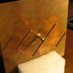
wifi biquad and card 2007
A biquad antenna for Wi-Fi, and a modified card to go with it.

miniPCI card hacking 2004
Bypassing HP's wireless whitelist for fun and profit.